
The PlayStation 5 DualSense controller has undergone several hardware revisions since its launch. This comprehensive technical guide covers all known revisions (BDM-010, BDM-020, BDM-030, BDM-040) with detailed schematics, pinout diagrams, and repair information for technicians and modders.
📌 Source Attribution
Technical information and images sourced from AcidMods Forum. This guide compiles and expands on community research for repair and modification purposes.
🎮 BDM-010: First Generation DualSense
The BDM-010 is the original DualSense revision featuring a 6-layer PCB. The primary hardware differences among early units were the FPC color (Blue or Green) and variations in TouchPad versions.
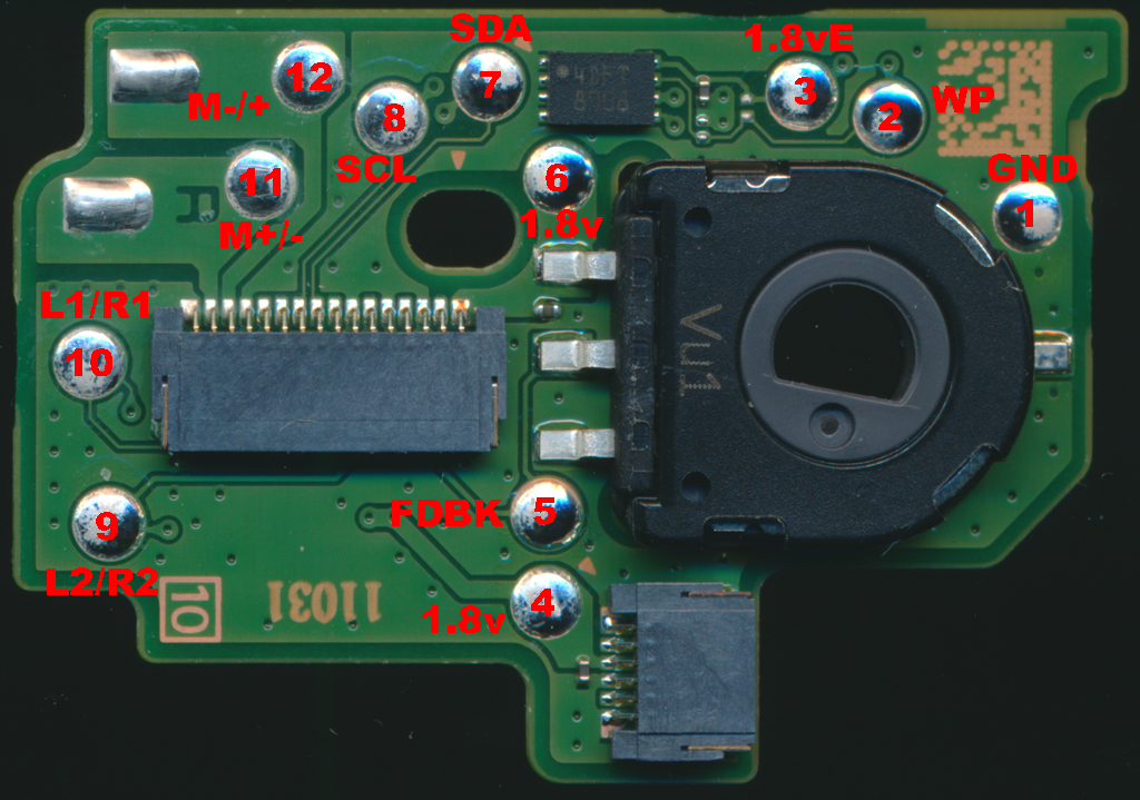
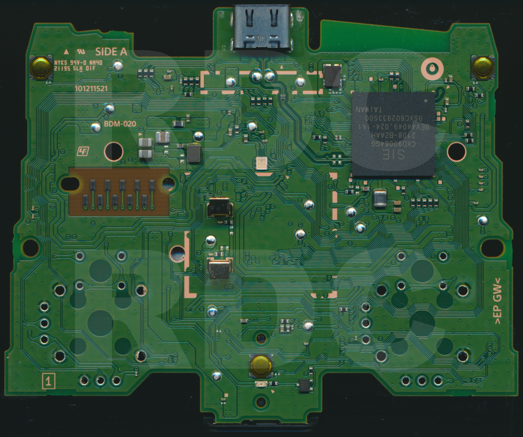
BDM-010 Motherboard PCB
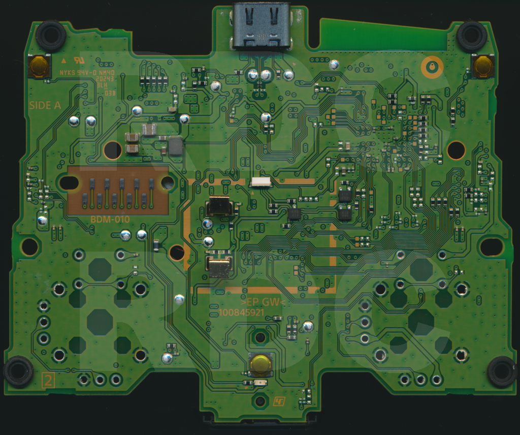
BDM-010 Motherboard - Top
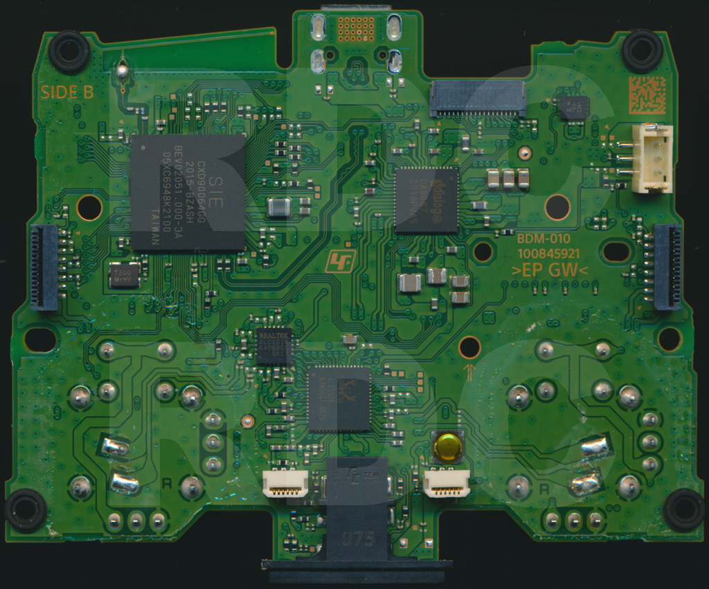
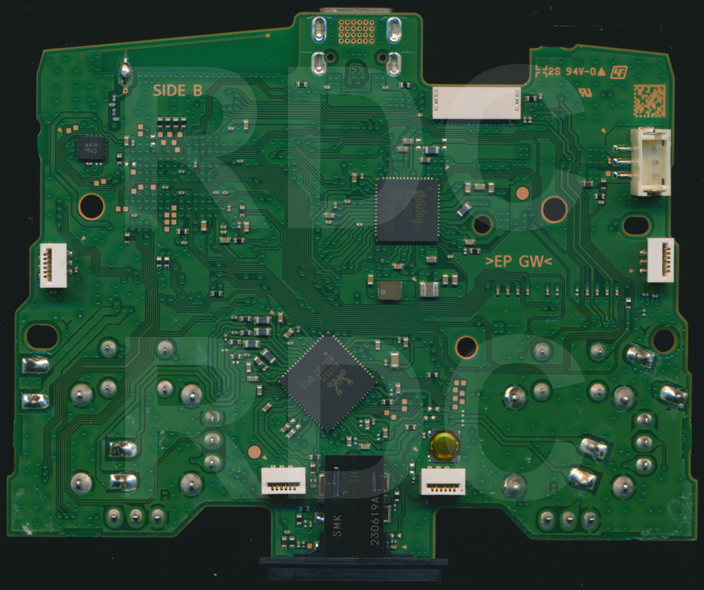
BDM-010 Motherboard - Bottom
BDM-010 Component Details
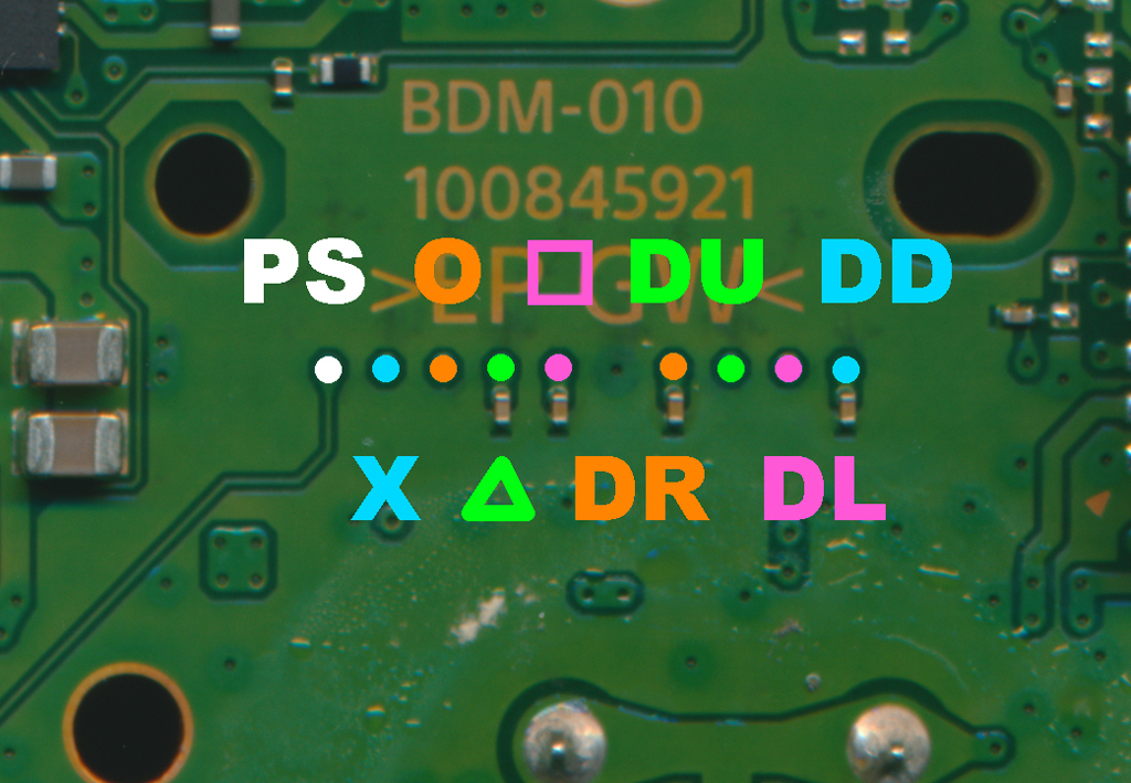
Button VIAs Layout
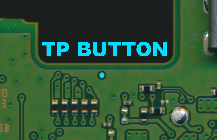
Touchpad & Button Details
Button Configuration
⚠️ IMPORTANT: Button Wiring Notes
- Most buttons: Common ground design
- L2 and R2: Voltage divider setup (analog)
- L3 and R3: Active Hi buttons - wire directly to solder joints if duplicating
- L1 and R1: Active Lo buttons
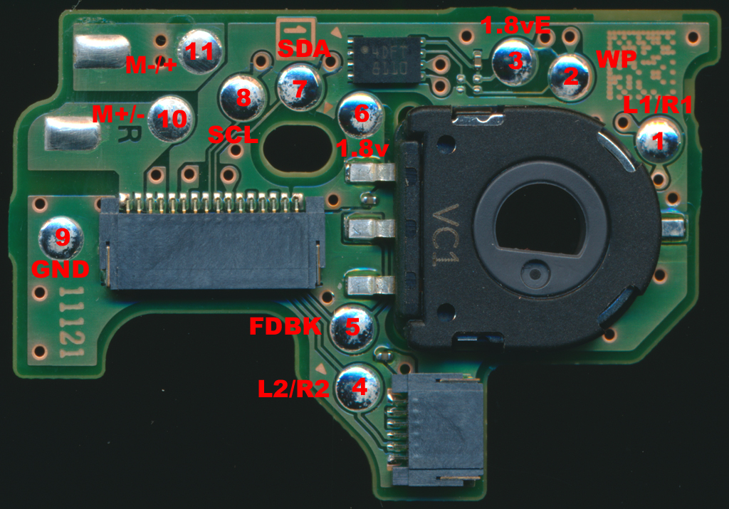
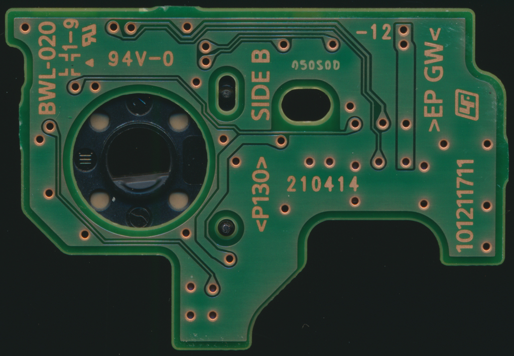
Trigger Assembly Details (BWL-010)
BWL-010 Trigger Assembly - Side A
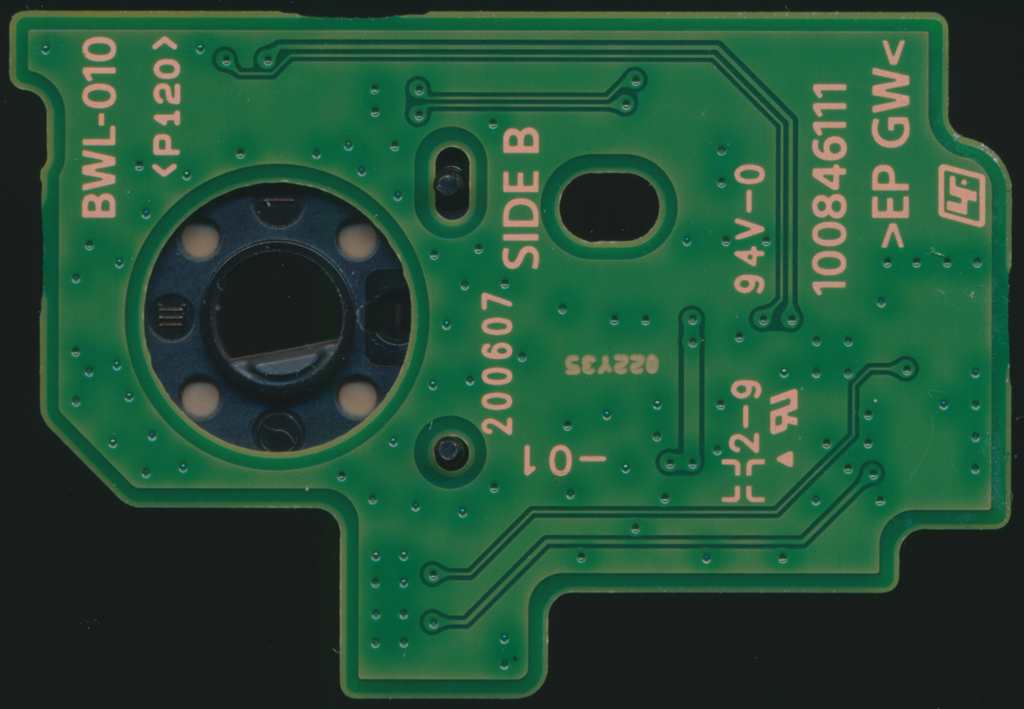
BWL-010 Trigger Assembly - Side B
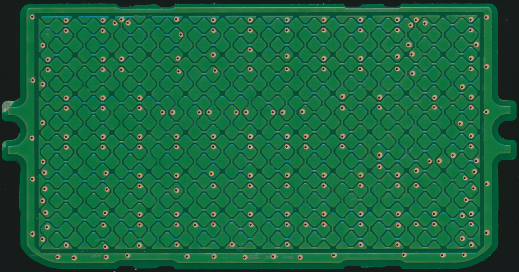
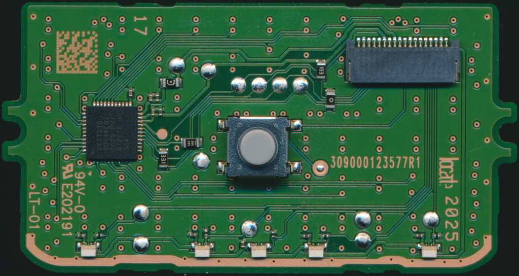
Touchpad Module (LT-01)
Touchpad Module - Top
Touchpad Module - Bottom
The L1/L2 and R1/R2 trigger assemblies are mechanically identical from a hardware standpoint, making the test point locations consistent across both sides.
⚠️ CRITICAL: FFC Connector Orientation
The Left and Right FFC connectors are placed 180° from each other, meaning their pinouts are reversed. Always verify which side you're working on before making connections!
LEFT SIDE FFC PINOUT (BDM-010)
| Pin | Function | Description |
|---|---|---|
| 1 | GND | Ground |
| 2 | M+/- | Motor Positive/Negative |
| 3 | M-/+ | Motor Negative/Positive |
| 4 | GND | Ground |
| 5 | 1.8vE | 1.8V EEPROM Power |
| 6 | WP2 | Write Protect (EEPROM) |
| 7 | SCL2 | I2C Clock (EEPROM) |
| 8 | SDA2 | I2C Data (EEPROM) |
| 9 | L1 | L1 Button Signal |
| 10 | GND | Ground |
| 11 | 1.8v | 1.8V Power |
| 12 | GND | Ground |
| 13 | L2 | L2 Analog Signal |
| 14 | GND | Ground |
| 15 | L2 Feedback | Force Feedback Position |
| 16 | 1.8v | 1.8V Power |
RIGHT SIDE FFC PINOUT (BDM-010)
| Pin | Function | Description |
|---|---|---|
| 1 | 1.8v | 1.8V Power |
| 2 | R2 Feedback | Force Feedback Position |
| 3 | GND | Ground |
| 4 | R2 | R2 Analog Signal |
| 5 | GND | Ground |
| 6 | 1.8v | 1.8V Power |
| 7 | GND | Ground |
| 8 | R1 | R1 Button Signal |
| 9 | SDA1 | I2C Data (EEPROM) |
| 10 | SCL1 | I2C Clock (EEPROM) |
| 11 | WP1 | Write Protect (EEPROM) |
| 12 | 1.8vE | 1.8V EEPROM Power |
| 13 | GND | Ground |
| 14 | M-/+ | Motor Negative/Positive |
| 15 | M+/- | Motor Positive/Negative |
| 16 | GND | Ground |
BWL-010 Trigger Board FFC Pinout
This is the pinout of the FFC connector on the BWL-010 trigger assembly board itself, NOT the motherboard connector.
| Pin | Function |
|---|---|
| 1 | 1.8v |
| 2 | L2/R2 Feedback |
| 3 | GND |
| 4 | L2/R2 |
| 5 | GND |
| 6 | 1.8v |
| 7 | GND |
| 8 | L1/R1 |
| 9 | SDA1 |
| 10 | SCL1 |
| 11 | WP1 |
| 12 | 1.8vE |
| 13 | GND |
| 14 | M- |
| 15 | M+ |
| 16 | GND |
EEPROM Mystery
🔍 Why Do Triggers Have EEPROMs?
The trigger assemblies contain integrated EEPROMs, likely for:
- Identification: Allowing the motherboard to recognize trigger assemblies
- Calibration Data: Storing force feedback calibration values
- Assembly Tracking: Manufacturing or quality control data
Recommendation: Leave EEPROM boards installed during repairs. Removing them may cause:
- Force feedback calibration issues
- Controller recognition problems
- Unknown side effects
The boards provide convenient test points once removed from the assembly housing while maintaining functionality.
L2/R2 Duplication Notes
⚠️ Important Wiring Instructions
When duplicating L2/R2 triggers:
- If trigger assembly is removed, install a Pull-Up Resistor from L2/R2 to 1.8V
- Connect new button from L2/R2 to Ground through a 1kΩ resistor
- Do NOT drive L2/R2 line directly to ground without resistance
- L2/R2 Feedback lines should not be left floating - more research needed on proper handling
I2C Lines Warning
The SDA, SCL, and WP lines are for EEPROM communication and should be left alone unless you know exactly what you're doing.
🎮 BDM-020: Second Generation DualSense
The second revision represents a significant change in PCB complexity while maintaining similar functionality. The BDM-020 introduces a 4-layer PCB design (reduced from 6 layers) to reduce manufacturing costs while preserving electrical compatibility.
BDM-020 Motherboard PCB
BDM-020 Motherboard - Top
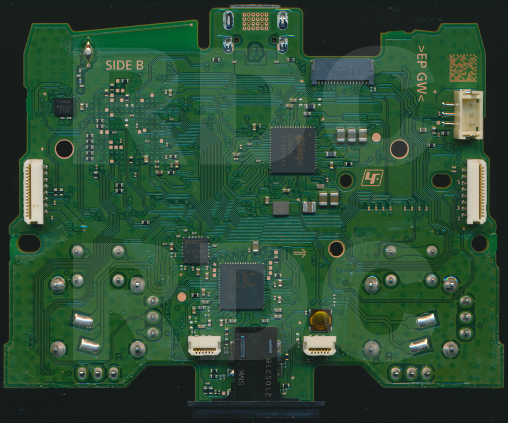
BDM-020 Motherboard - Bottom
BWL-020 Trigger Assembly
BWL-020 Trigger Assembly - Top
BWL-020 Trigger Assembly - Bottom
Key Changes from BDM-010
- PCB Layers: Reduced from 6-layer to 4-layer design
- Button VIAs: Face buttons (PS, X, O, △, □) and D-Pad maintain same locations as BDM-010
- Trigger Assemblies: Mechanically identical to BDM-010 but with relocated test points
BWL-020 Trigger Assembly
The trigger hardware remains functionally the same, but test point locations have been repositioned on this revision. Refer to visual guides for exact TP locations.
⚠️ Test Point Relocation
While the trigger assemblies work identically to BDM-010, the physical location of test points has changed. Always verify TP locations visually before soldering.
🎮 BDM-030: Third Generation DualSense
The third revision introduces the most significant architectural change to the trigger system. This generation simplifies the trigger design while maintaining adaptive trigger functionality through direct motor wiring.
BDM-030 Motherboard PCB
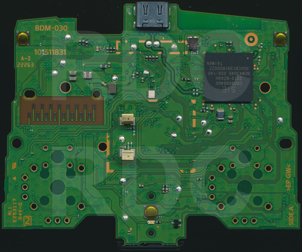
BDM-030 Motherboard - Top
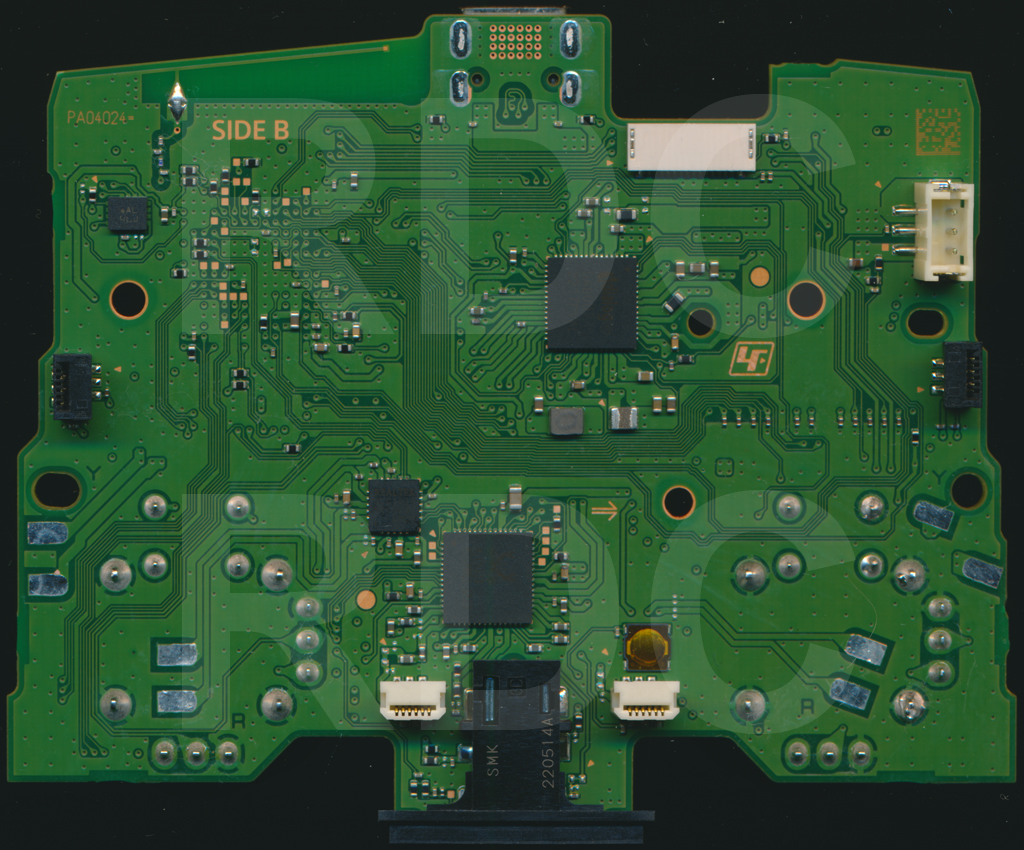
BDM-030 Motherboard - Bottom
BDM-030 FPC Button Assembly
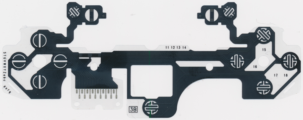
BDM-030 FPC - Integrated Button Assembly
Flexible PCB with integrated L1, L2, R1, R2 button contacts
Major Trigger Assembly Redesign
- Simplified PCB: Trigger boards now only contain the Feedback POT
- Direct Motor Connection: Feedback motors wired directly to motherboard (like rumble motors)
- Integrated FPC: L1, L2, R1, and R2 buttons now incorporated into the FPC
- Classic Design: Returns to DS4, DS3, and DS2 style trigger implementation
📋 Design Philosophy Shift
Sony simplified the trigger assembly design significantly in BDM-030, potentially for:
- Reduced manufacturing complexity
- Lower production costs
- Improved reliability
- Easier assembly/disassembly
BDM-030 FPC Details
The new FPC design integrates button contacts directly into the flexible PCB, eliminating separate trigger board assemblies for button switching.
🎮 BDM-040: Fourth Generation DualSense
The latest known revision continues the design philosophy established in BDM-030 with further refinements and optimizations.
BDM-040 Motherboard PCB
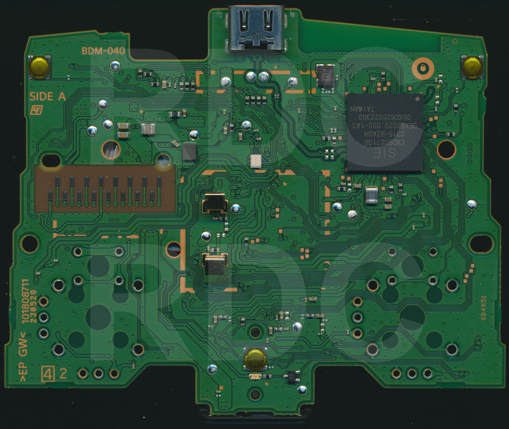
BDM-040 Motherboard - Top
BDM-040 Motherboard - Bottom
Current Status
Details on specific changes in BDM-040 are still being documented. The revision appears to maintain the BDM-030 trigger assembly design with possible component or layout optimizations.
🔧 Repair and Modification Guidelines
General Best Practices
- Identify Your Revision: Check motherboard marking (BDM-010/020/030/040) before starting work
- Document Before Disassembly: Take photos of cable routing and connector orientations
- Verify Pinouts: Always confirm FFC orientation - left and right connectors are reversed!
- Test Before Reassembly: Verify all functions before fully closing the controller
- EEPROM Preservation: Keep trigger EEPROMs installed when possible (BDM-010/020)
Common Repair Scenarios
Trigger Drift or Dead Zones
- Check L2/R2 analog potentiometer for wear
- Clean potentiometer contacts with isopropyl alcohol
- Replace POT if mechanically damaged
- Verify feedback motor connections
Non-Responsive Buttons
- Test button continuity at VIA points
- Check for damaged FPC contacts
- Verify proper FFC seating in connectors
- Inspect for torn or cracked flexible cables
Force Feedback Issues
- Verify motor power connections
- Check feedback POT resistance values
- Ensure EEPROM is properly connected (BDM-010/020)
- Test motor driver circuit on motherboard
🛠️ Required Tools and Equipment
Essential Tools
- Soldering Iron: Temperature-controlled, fine tip (0.5mm recommended)
- Multimeter: For continuity and voltage testing
- Hot Air Station: For component-level repairs
- Precision Screwdrivers: Phillips #00 and #000
- Spudgers: Plastic pry tools for shell separation
- Tweezers: Fine-point ESD-safe tweezers
Consumables
- Leaded solder (63/37 or 60/40)
- Flux paste or pen
- Isopropyl alcohol (90%+ purity)
- Kapton tape
- Resistors (1kΩ for button mods)
⚠️ Safety and Precautions
🔴 Critical Safety Information
- ESD Protection: Use anti-static wrist strap when handling PCBs
- Battery Safety: Disconnect battery before any electrical work
- Heat Sensitivity: Keep soldering iron below 350°C for FPC work
- Component Polarity: Verify component orientation before installation
- Voltage Verification: Double-check all voltage levels with multimeter
- No Warranty: Modifications and repairs void Sony warranty
📝 Conclusion
The DualSense controller has evolved significantly through four major hardware revisions, each bringing improvements in manufacturing efficiency and design optimization. Understanding these differences is crucial for successful repairs and modifications.
Key takeaways:
- BDM-010 features complex 6-layer PCB with EEPROM-equipped trigger assemblies
- BDM-020 simplified to 4-layer while maintaining button layout compatibility
- BDM-030/040 adopted integrated FPC design, eliminating separate trigger boards
- Always verify revision number before starting repairs
- FFC connectors are reversed between left and right sides
- Preserve EEPROMs when working with BDM-010/020 triggers
🔧 Professional Repair Services
Need help with your DualSense controller repair? Akku Electronics in Nagpur offers professional PlayStation controller repair services with expertise in all DualSense revisions.
📚 References and Resources
Primary PCB Schematic Sources
- AcidMods Forum - DualSense PCB Scans Thread
The definitive resource for high-resolution PCB layouts, pinout diagrams, and schematic information for all DualSense revisions (BDM-010, 020, 030, 040). Includes detailed component locations and test points.
Related Articles
- 15 DualSense Tips & Tricks You Need to Know - Practical modification and customization guides
- PS5 Pro Technical Analysis - Controller hardware innovations
Professional Services
- Akku Electronics Repair Services - Expert DualSense repair, modification, and customization in Nagpur, India
Disclaimer
⚠️ Caution: All repairs and modifications are performed at your own risk. Improper soldering, component damage, or modification errors can permanently damage your controller and void warranty. Always verify your hardware revision before attempting modifications. Refer to the AcidMods forum scans for precise component locations. When in doubt, consult professional repair services.